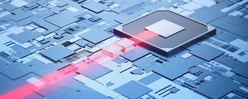
Economical, Scalable Manufacturing of Integrated Photonic and Array Devices
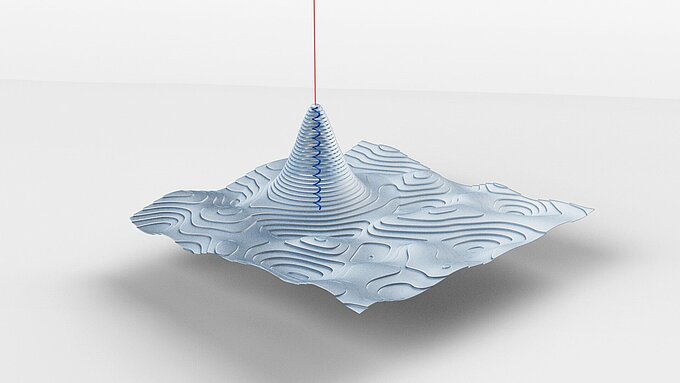
Providing immense transmission capacity with low energy consumption, optical communication is the driving force of communication networks. Placing optical components on wafers of silicon and other substrates and creating optical connections are recurring process steps in the production and quality assurance of silicon photonic components and photonic integrated circuits (PICs). Often, very stringent transverse tolerances are required, making precision, velocity, and a high degree of automation of the alignment indispensable for the functionality and cost of manufacturing components and PICs.
Eliminating the Primary Cost Driver in PIC Production
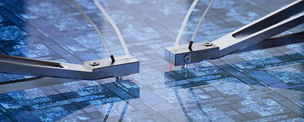
For silicon photonics (SiPh) device manufacturing from wafer level to assembly to packaging, alignment time is the primary cost driver. For wafer-level testing, this applies to engineering probers and even more so to production probers, for which uptime and throughput are especially critical. With their advanced autonomous alignment functionality and fab-qualified mechanics, photonics alignment algorithms and subsystems from PI meet the demanding needs of the industry by providing unmatched speed, throughput, and accuracy with gains of several orders of magnitude over traditional alignment technologies. In photonic packaging, the alignment of optical fibers, waveguides, and other components must be meticulously controlled. Our expertise in array alignment allows us to provide solutions that meet the stringent demands of silicon photonics applications. By leveraging advanced positioning systems and alignment algorithms, we enable superior performance and reliability.
Integrated Solutions for Challenging Silicon Photonics Applications
From quality assurance for optical devices and components at wafer level, to chip testing, to final assembly and packaging, PI offers comprehensive and diverse solutions for different chip designs, formats, and tasks.
Your Advantages with PI as Partner
- Motion control systems designed to enhance the speed and accuracy of the photonics alignment process using advanced technologies
- PI motion control and alignment algorithms providing unique ways to find first light, to characterize a coupling, and to simultaneously align multiple inputs and outputs
- Close collaboration with our clients—to understand your unique requirements and provide customized solutions that meet your specific needs
- Team of specialists with decades of experience in developing and implementing motion control systems and photonics alignment solutions
- Design, production, and service centers in North America, Asia, and Europe to accelerate your next project