In the last decades, optical limitations of light-based microscopy have been overcome with several super-resolution techniques, such as light-sheet microscopy, where precision motion control equipment plays a key role.
Even higher resolution can be achieved with high-resolution physical scanning (i.e. scanning probe microscopy, or SPM), where nano-positioning systems become essential.
Atomic force microscopy (AFM), for example, is an advanced method of measuring the 3D surface topology of samples on the sub-nanometer scale. This level of resolution exceeds the optical diffraction limit of the conventional compound microscope by over 1,000 times, necessitating the use of ultra-precise nano-positioning systems to acquire accurate measurement data from sample scanning.
In this blog post, PI explores some of the principles of AFM in more detail. We will also outline some of our nano-positioning systems which have proven instrumental in the growing success of high-technology AFM studies.
Working Principles of AFM
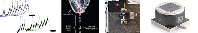
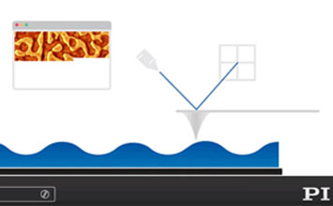
Central to any AFM is the surface sensing probe, which consists of an extremely sharp tip (with a radius on the order of nanometers) attached to the end of a rectangular cantilever. There are several modes of operation, but for the sake of simplicity, we will only discuss contact mode in this article.
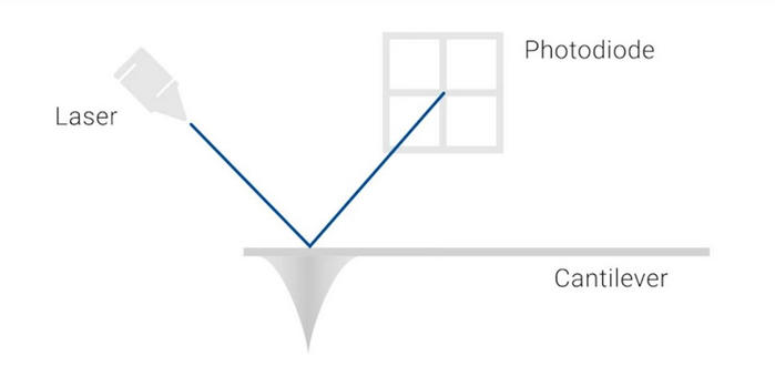
Contact mode AFM brings the probe tip into proximity with the surface of a sample which is mounted on a nano-positioning system, such as a piezo stage. This stage moves the sample with multi-axis control (X, Y, Z axes) relative to the tip apex, and helps to maintain a constant tip-sample interaction force as the surface is scanned. The reason this interaction force changes is most commonly due to topological variations, though it may be indicative of any number of complex phenomena occurring at the sub-nanoscale (ferroelectrics for example). An integrated photodiode continually monitors these changes by measuring the position of the cantilever, which bends in response to the Z-orbit of the tip. Probing these sub-nanometer surface variations provides valuable insights for materials characterizations in a broad range of fields.
Nano-Positioning Systems in AFMs
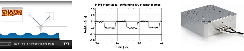
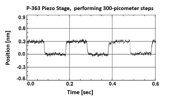
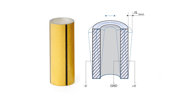
AFM’s can be designed in different ways. It is common to scan the tip, which is often done with piezo scanner tubes. These tubes are relatively low cost and simple, but are limited in scan range and linearity. Higher precision can be achieved with flexure guided piezo nano-positioning stages used to scan the sample instead of the tip. Piezo stages with capacitive feedback - which means that capacitive sensors actively provide nanometer precise position control of the piezo stage - can achieve lateral and Z-axis resolutions down to 0.1 nanometers, excellent prerequisites for both atomic force and near-field microscopy. This is true even for sample stages used for measurements of comparatively high lateral scanning ranges – up to 100µm and more, in AFM and confocal Raman microscopy.
By combining a very large scanning range with unique levels of precision, piezo-based nano-positioning systems are ideal for achieving high-resolution imaging of even large sample areas. Large sample measuring has long been a pain point for AFMs, as large sample measurements typically sacrifice scanning speeds in favor of precision. Partially responsible for this are the poor dynamics of conventional nano-positioning systems, which are incapable of combining few nanometre resolutions with larger travel ranges.
AFM and Optical Microscopy Combined
It is also possible to combine scanning optical and scanning force microscopy to gain even more information on the samples.
Nano-Positioning Systems from PI
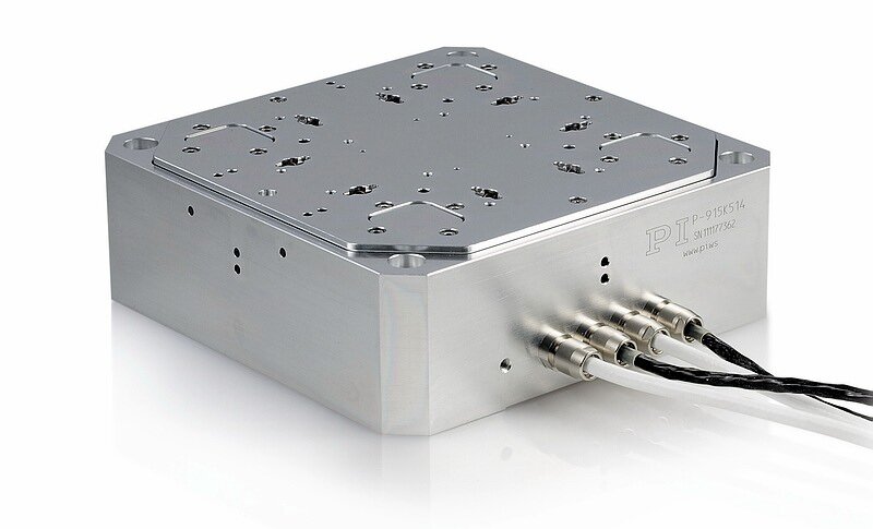
PI specializes in the provision of high-performance nano-positioning systems for rapid and high-accuracy AFMs. Our product line offers unmatched specimen positioning capabilities with rapid response times and outstanding multi-axis precision, with sub-nanometre resolution, the highest possible linearity, and exceptional scanning flatness. This range includes:
- P-517, P-527 and P-563 Multi-Axis Piezo Scanner
- P-363 PicoCube XY(Z) Piezo Scanner with Sub-Nanometer Resolution
- P-313 PicoCube XY(Z) Piezo Scanner with Sub-Nanometer Resolution
If you are interested in the capabilities of any of the above nano-positioning systems, simply contact a member of the PI team today.